We’ve been hearing rumors about a ChatGPT search engine for a while now, but now it's finally live. Rather than being a whole new website called 'SearchGPT', as many had expected, it’s simply an upgrade to the existing ChatGPT website, and all the ChatGPT apps for Windows, Mac, and smartphones.
When you are talking to ChatGPT it will now ask you if it should search the web, if it feels that would produce better results for you, but you can also manually instigate a web search at any time. As you’d expect, ChatGPT search is a feature that’s available immediately for ChatGPT Plus subscribers, and all ChatGPT Plus and Team users will get it today. However, all SearchGPT waitlist users will also be getting access today. Enterprise and Edu users of ChatGPT will be getting access over the next few weeks.
A new Citations bar will open on the right of the window when you click a source link.(Image credit: OpenAI)
How it works
If you look at your ChatGPT prompt bar you’ll see a new search icon called Search. Tap or click this and you will be searching the web using ChatGPT, rather than engaging in a conversation. It’s a bit like the AI summaries that Google already provides in its search engine, but there is an easily identifiable link to sources after each piece of text. When clicked, the sources open up a sidebar that shows citations.
In case you were wondering, the waitlist for SearchGPT is now closed, so if you haven’t already signed up, it’s now too late. As for when the rest of the ChatGPT free tier will get it, OpenAI says, “We’ll roll out to all Free users over the coming months.”
ChatGPT search is perfect for all the jobs you'd normally use Google for.(Image credit: OpenAI)
What's interesting is that ChatGPT has partnered with various industry sources to provide its own maps, that aren't Google Maps, as well as weather, stocks, sports, and news information. OpenAI says it has "partnered with news and data providers to add up-to-date information and new visual designs for categories like weather, stocks, sports, news, and maps."
ChatGPT Search is already looking enticing and could be the first real threat to Google in years. With ChatGPT Search, you’re essentially getting the natural language capabilities of ChatGPT blended with up-to-the-minute information from the web, and that could be just what people are searching for.
Bandwidth limitations have become a significant bottleneck in AI and high-performance computing (HPC), as GPUs are underutilized due to bandwidth constraints, with nearly half of their computational power going to waste.
Nvidia is not expected to release optical interconnects for its NVLink protocol until the "Rubin Ultra" GPU compute engine launches in 2027.
This delay has led hyperscalers and cloud builders to explore ways to leapfrog Nvidia’s technology by adopting optical interconnects earlier.
Introducing ChromX
Xscape Photonics, an optical interconnect company spun out of research at Columbia University, is using photonics to realize scalable, high-bandwidth, energy-sustainable, and cost-effective solutions to enable the next generation of AI, ML, and simulation hardware.
This could help the AI industry save billions of dollars in wasted GPU capacity while also offering a path to greener, more sustainable AI infrastructures.
The Next Platform recently took a closer look at Xscape Photonics and spoke with the team behind it, including CEO Vivek Raghunathan, a former MIT researcher and Intel engineer.
Raghunathan highlighted the inefficiencies of current GPU systems, explaining that as scaling continues, the problem shifts "from GPU device-level performance to a system-level networking problem."
This is where Xscape’s technology comes into play. By converting electrical signals into optical ones directly within the GPU, Xscape can dramatically increase bandwidth while simultaneously reducing power consumption.
The startup’s solution, called the "ChromX" platform, uses a laser that can transmit multiple wavelengths of light simultaneously through a single optical fiber - up to 128 different wavelengths (or "colors"). This enables a 32-fold increase in bandwidth compared to lasers that use only four wavelengths.
The ChromX platform also relies on simpler modulation schemes like NRZ (Non-Return-to-Zero), which reduce latency compared to higher-order schemes like PAM-4 used in other systems such as InfiniBand and Ethernet. The ChromX platform is programmable, allowing it to adjust the number of wavelengths to match the specific needs of an AI workload, whether for training or inference tasks.
Raghunathan told The Next Platform’s Timothy Prickett Morgan, “The vision is to match in-package communication bandwidth to off-package communication escape bandwidth. And we think when we use our multicolor approach, we can match that so that giant datacenters - or multiple datacenters - behave as one big GPU.”
The potential impact of this technology is enormous. AI workloads consume vast amounts of energy, and with data center demand projected to triple by 2035, power grids may struggle to keep up. Xscape Photonics’ innovations could offer a vital solution, enabling AI systems to operate more efficiently and sustainably.
A leading expert has raised critical questions about the validity of claims surrounding "Zettascale" and "Exascale-class" AI supercomputers.
In an article that delves deep into the technical intricacies of these terms, Doug Eadline from HPCWire explains how terms like exascale, which traditionally denote computers achieving one quintillion floating-point operations per second (FLOPS), are often misused or misrepresented, especially in the context of AI workloads.
Eadline points out that many of the recent announcements touting "exascale" or even "zettascale" performance are based on speculative metrics, rather than tested results. He writes, "How do these 'snort your coffee' numbers arise from unbuilt systems?" - a question that highlights the gap between theoretical peak performance and actual measured results in the field of high-performance computing. The term exascale has historically been reserved for systems that achieve at least 10^18 FLOPS in sustained, double-precision (64-bit) calculations, a standard verified by benchmarks such as the High-Performance LINPACK (HPLinpack).
Car comparison
As Eadline explains, the distinction between FLOPS in AI and HPC is crucial. While AI workloads often rely on lower-precision floating-point formats such as FP16, FP8, or even FP4, traditional HPC systems demand higher precision for accurate results.
The use of these lower-precision numbers is what leads to inflated claims of exaFLOP or even zettaFLOP performance. According to Eadline, "calling it 'AI zetaFLOPS' is silly because no AI was run on this unfinished machine."
He further emphasizes the importance of using verified benchmarks like HPLinpack, which has been the standard for measuring HPC performance since 1993, and how using theoretical peak numbers can be misleading.
The two supercomputers that are currently part of the exascale club - Frontier at Oak Ridge National Laboratory and Aurora at Argonne National Laboratory - have been tested with real applications, unlike many of the AI systems making exascale claims.
To explain the difference between various floating-point formats, Eadline offers a car analogy: "The average double precision FP64 car weighs about 4,000 pounds (1814 Kilos). It is great at navigating terrain, holds four people comfortably, and gets 30 MPG. Now, consider the FP4 car, which has been stripped down to 250 pounds (113 Kilos) and gets an astounding 480 MPG. Great news. You have the best gas mileage ever! Except, you don’t mention a few features of your fantastic FP4 car. First, the car has been stripped down of everything except a small engine and maybe a seat. What’s more, the wheels are 16-sided (2^4) and provide a bumpy ride as compared to the smooth FP64 sedan ride with wheels that have somewhere around 2^64 sides. There may be places where your FP4 car works just fine, like cruising down Inference Lane, but it will not do well heading down the FP64 HPC highway."
Eadline’s article serves as a reminder that while AI and HPC are converging, the standards for measuring performance in these fields remain distinct. As he puts it, "Fuzzing things up with 'AI FLOPS' will not help either," pointing out that only verified systems that meet the stringent requirements for double-precision calculations should be considered true exascale or zettascale systems.
If you want to buy a MacBook Air but your budget won’t quite stretch, Infinix has launched a lightweight, highly-affordable Windows 11 alternative which brings an impressive array of features promising to rival higher-end competitors.
The Inbook Air Pro+ weighs only 1kg, placing it firmly in the thin and light category - ideal for everyday use, performance, processing, and multitasking.
Equipped with Intel’s 13th Gen Core i5 processor (1334U), featuring 10 cores, a 4.6GHz turbo boost, and integrated Iris Xe graphics, the laptop comes with 16GB of LPDDR4X RAM and 512GB of M.2 NVMe SSD storage - doubling the memory and storage capacity of the entry-level MacBook Air. An advanced cooling system with 79 precision-designed 0.2mm S-shaped fan blades prevents the device from overheating when under load.
Short battery life
One of the highlights of the Air Pro+ is its 14-inch OLED 2.8K (2880 x 1800) display. It’s rare to see an OLED panel at this price, so that alone is a great selling point. With a 16:10 aspect ratio, a peak brightness of 440 nits, and a 120Hz refresh rate, it promises vibrant, sharp visuals. The display also supports 100% of both the sRGB and DCI-P3 color gamuts, ensuring accurate color reproduction - ideal for creative professionals.
The Air Pro+ sports all the ports you expect to see on a modern laptop, such as USB-C, HDMI 1.4, and USB 3.2. It also comes with a Full HD+ IR webcam supporting face recognition and a backlit keyboard. Wireless connectivity is provided in the form of WiFi 6 and Bluetooth 5.2.
The 57Wh battery life, as per Infinix’s claims, lasts up to 8–10 hours, which should be just enough to get you through a full workday. In comparison, the Apple MacBook Air offers up to 18 hours. The Air Pro+ does at least support 65W Type-C fast charging.
Currently priced at 49,990 Indian rupees (approximately $600) on Flipkart, the Infinix Air Pro+ provides impressive specs for its price, offering a tempting option for budget-conscious buyers who need performance and portability without breaking the bank.
Japan is often seen as a global leader in cutting-edge technology, known for innovations in robotics, electronics, and high-speed trains - however, the country is also known for its tendency to hold onto older technology long after it has been abandoned elsewhere.
Only recently has Japan begun to phase out floppy disks in government offices, and far too many of its laptops and devices still come equipped with legacy features like VGA connectors. Most recently, we covered a PCI Express adapter that adds a parallel port to modern PCs, allowing buyers to connect long-forgotten devices like HP LaserJet or dot matrix printers. For bonus nostalgia points, the driver for it comes on a CD, and it’s compatible with Windows XP and newer.
But now, Planex Communications has embraced Japan’s unwillingness to fully move on with the release of its PL-US56K2(A) USB-connected 56K modem, ideal for anyone who still needs to dial into the internet like it’s 1999.
For around 5,980 yen (about $40) on Amazon, this device is designed for PCs without built-in modems, enabling access to analog public phone lines for internet connectivity, data transmission, and even faxing - all without needing to install any drivers.
The modem supports the ITU-T V.90 and V.92 protocols, offering a maximum theoretical data reception speed of 56Kbps and a transmission speed of up to 33.6Kbps. At those speeds, you won’t be streaming HD videos, but you can at least check your emails or send a fax while reflecting on how far technology has come - or hasn’t, depending on your perspective.
Powered via USB 2.0, the PL-US56K2(A) is small and light, weighing just 28 grams and measuring a compact 25mm x 75mm x 18mm, making it easy to tuck away next to your other relics from the late '90s like your floppy disks, PalmPilot, and that stack of AOL free trial CDs.
The PL-US56K2(A) isn’t likely to take the world by storm, but it’s a handy solution for anyone still navigating the world of dial-up or needing to send the occasional fax.
A new leak claims AMD’s upcoming Ryzen 7 9800X3D processor will see an 8% performance boost over the Ryzen 9 7800X3D — in other words, the chip that is regarded as one of the best gaming CPUs on the market now looks set to be dethroned.
This could stand as a significant boost for PC gamers, especially considering the improvement in 3D V-Cache, which was a downside in our AMD Ryzen 7 7800X3D review. The leak from VideoCardz contains a marketing description of the 9800X3D, revealing ‘Next-Gen 3D V-Cache’ which points towards better thermal performance when operating at higher clock speeds.
VideoCardz also reports that it’s expected to have a 15% enhancement over the 7800X3D in multi-threaded workloads, ideal for multi-tasking duties and video editing, using 8 cores and 16 threads — this strikes a balance for both content creators and gamers, along with the aforementioned 3D V-Cache improvements. These pivotal enhancements being leaked ahead of the 9800X3D’s confirmed November 7th launch and AMD’s full spec reveal gives gamers some insight into what to expect.
Will the 9800X3D be worth the upgrade?
While we have yet to see the full scope of what the Ryzen 7 9800X3D will have to offer specification-wise, the leaked marketing description gives us a great idea of what is in store for PC gamers. Considering the aforementioned 8% boost in gaming performance and room for slightly higher clock speeds up to 5.2GHz compared to the previous 5GHz, the switch is certainly worth contemplating - and for gamers who have yet to upgrade to an AM5 chip, this performance boost could finally be the push they need.
Despite the improvements listed in the leak, it’s important to note that there is only so much that can be done when it comes to poor game optimization on PC — an upgrade can help specifically with reducing stuttering in certain games, but it’s not the silver bullet for achieving optimal performance. Besides, most modern games are far more dependent on your GPU and available VRAM.
If you’re using the best GPUs on the market, like the Nvidia RTX 4080 Super or RTX 4090, any kind of upgrade isn’t entirely urgent, but we’ll have to wait to see everything AMD’s new processor has to offer before we can pass judgment on the value of this new chip.
Back in March 2024, we reported how British AI startup Literal Labs was working to make GPU-based training obsolete with its Tseltin Machine, a machine learning model that uses logic-based learning to classify data.
It operates through Tsetlin automata, which establish logical connections between features in input data and classification rules. Based on whether decisions are correct or incorrect, the machine adjusts these connections using rewards or penalties.
Developed by Soviet mathematician Mikhail Tsetlin in the 1960s, this approach contrasts with neural networks by focusing on learning automata, rather than modeling biological neurons, to perform tasks like classification and pattern recognition.
Energy-efficient design
Now, Literal Labs, backed by Arm, has developed a model using Tsetlin Machines that despite its compact size of just 7.29KB, delivers high accuracy and dramatically improves anomaly detection tasks for edge AI and IoT deployments.
The model was benchmarked by Literal Labs using the MLPerf Inference: Tiny suite and tested on a $30 NUCLEO-H7A3ZI-Q development board, which features a 280MHz ARM Cortex-M7 processor and doesn’t include an AI accelerator. The results show Literal Labs’ model achieves inference speeds that are 54 times faster than traditional neural networks while consuming 52 times less energy.
Compared to the best-performing models in the industry, Literal Labs’ model demonstrates both latency improvements and an energy-efficient design, making it suitable for low-power devices like sensors. Its performance makes it viable for applications in industrial IoT, predictive maintenance, and health diagnostics, where detecting anomalies quickly and accurately is crucial.
The use of such a compact and low-energy model could help scale AI deployment across various sectors, reducing costs and increasing accessibility to AI technology.
Literal Labs says, “Smaller models are particularly advantageous in such deployments as they require less memory and processing power, allowing them to run on more affordable, lower-specification hardware. This not only reduces costs but also broadens the range of devices capable of supporting advanced AI functionality, making it feasible to deploy AI solutions at scale in resource-constrained settings.”
A new variant of the infamous ClearFake (AKA ClickFix) malware has been detected in the wild, and has already managed to compromise thousands of WordPress websites.
Researchers from GoDaddy claim to have spotted a variant of this campaign, which installs malicious plugins to sites on the website builder. The threat actors would use the credentials stolen elsewhere (or bought on the black market) to log into the website’s WordPress admin account, and install a seemingly benign plugin.
The victims are then enticed to download an update, which is just a piece of malware that steals sensitive data, or does something else but equally sinister.
Thousands of compromised websites
In turn, the plugin displays the various popups, requesting the victims do different actions (all of which lead to the installation of infostealers).
The entire process is automated, GoDaddy is saying, and so far more than 6,000 WordPress websites have fallen prey.
"These seemingly legitimate plugins are designed to appear harmless to website administrators but contain embedded malicious scripts that deliver fake browser update prompts to end-users,” the researchers are saying. The plugins are “seemingly legitimate” as they carry household names in the WordPress world, such as Wordfense Security, or LiteSpeed Cache.
Here is the full list of the plugins spotted so far:
LiteSpeed Cache Classic
MonsterInsights Classic
Wordfence Security Classic
Search Rank Enhancer
SEO Booster Pro
Google SEO Enhancer
Rank Booster Pro
Admin Bar Customizer
Advanced User Manager
Advanced Widget Manage
Content Blocker
Universal Popup Plugin
ClearFake is a type of malware attack we’ve all seen in the past - a website is compromised and used to display a fake popup notification. This notification usually mimics an antivirus warning, or a browser notification, and informs the user that their computer is either infected with a virus, or outdated and therefore unable to display the desired website.
The OnePlus 13 is set to be one of the final flagship phones of 2024, though it will probably only be a 2024 release in China, with the rest of the world likely to get it in 2025.
Either way though, it could be worth the wait, as between leaks and teasers we have a good idea of what to expect, and that includes an extremely powerful and efficient chipset, a huge battery, and a striking design.
Below then, you’ll find everything we’ve heard about the OnePlus 13 so far, including its confirmed announcement date and design, and leaked specs and features.
Cut to the chase
What is it? The next OnePlus flagship
When is it out? October 31 in China, maybe early next year globally
How much will it cost? Likely upwards of $799.99 / £849 (around AU$1,200)
A rumored price increase
The OnePlus 12(Image credit: Philip Berne / Future)
Landing in China on October 31
Could cost more than the OnePlus 12
The OnePlus 13 will be unveiled on October 31 at an event in China. The company itself has confirmed this, with the event kicking off at 1am PT / 4am ET / 8am GMT / 7pm AEDT.
This event will most likely just be the Chinese launch of the phone though, with a global launch probably happening in early 2025 based on past form.
The OnePlus 13 might also cost more than the OnePlus 12, with one leak suggesting a 16GB model with 512GB of storage will cost ¥5,299 in China, which is up from ¥4,799 for the equivalent model of the OnePlus 12. That’s a difference of around $70 / £55 / AU$105.
For reference, the OnePlus 12 cost $799.99 / £849 (around AU$1,200) at launch for a 12GB / 256GB model, and rose to $899.99 / £999 (roughly AU$1,350) for a 16GB / 512GB version. So the OnePlus 13 might have a higher price than that.
Oh, and don’t count on being able to buy it in Australia, because the current model isn’t available there.
Can you trust these rumors?
We've only heard one price leak so far so we'd take it with a pinch of salt. But it's believable that the OnePlus 13 would cost more than the OnePlus 12, especially as the Snapdragon chipset we're expecting it to use reportedly costs more than its predecessor.
A familiar design and a new screen technology
The OnePlus 12(Image credit: Philip Berne / Future)
A familiar design in new colors
The screen has an interesting refresh rate technology
The phone will be available in White Dawn (white), Blue Moment (blue), and Obsidian Secret (black) shades, with the blue one apparently having a skin-like feel and the black one having an “ebony wood grain” textured finish.
The design of the back otherwise looks somewhat similar to the OnePlus 12, but the circular camera block doesn’t extend out to the edge here, and instead there’s a silver line running across the rear.
The OnePlus 13 in three colors(Image credit: OnePlus)
We haven’t yet had a complete official look at the front of the phone, but you can see glimpses of it in a OnePlus 13 teaser video, showing what appears to be a flat display with a punch-hole camera in the top center.
We’ve also seen actual photos of the OnePlus 13, from where it was spotted at a Chinese esports event, as you can see below.
Images of the OnePlus 13 at an esports event(Image credit: Weibo)
Still, it shows a seemingly flat screen with a punch-hole camera, similar to other teasers above.
A possible image of the OnePlus 13(Image credit: OnePlus)
In any case, leaks suggest the OnePlus 13 might have a 6.82-inch display, which is the same as the OnePlus 12. An early leak also suggested the OnePlus 13 would have a curved screen, but based on more recent leaks and teasers that doesn’t appear to be the case, unless it’s a very subtle curve.
The company has also teased on Weibo that its screen will be able to deliver different refresh rates in different sections, so for example static text could be at 10Hz while a video playing elsewhere on the screen could be 120Hz. This is something we haven’t seen from other Android phones, and it might allow for improved battery life.
Most of the design has now been confirmed, and the leaked screen specs are all in line with what we'd expect. The one real question mark here is whether the OnePlus 13 will have an ultrasonic fingerprint sensor, but it sounds believable.
A mix of old and new cameras
The OnePlus 12(Image credit: Philip Berne / Future)
It would be a shame not see any upgrades there, but in an earlier leak the same source claimed OnePlus was working on the OnePlus 13’s periscope camera, so that at least might differ from the 64MP 3x zoom of its predecessor.
As for exactly how it might differ, well, both that source (Digital Chat Station, via Android Authority) and leaker Yogesh Brar have claimed that the OnePlus 13 might have three 50MP cameras. In which case that would also mean changes to the ultra-wide, as that’s 48MP on the OnePlus 12.
Can you trust these rumors?
The cameras are one of the things we're least sure about, as we haven't heard all that much about them. But the leaks we have heard generally all point in the same direction, so the specs above have a good chance of being accurate.
An efficient chipset and a huge battery
The OnePlus 12(Image credit: Philip Berne / Future)
That should help improve battery life, as should the ability to deliver different refresh rates to different parts of the screen, as mentioned further up in this article. And that’s on top of the OnePlus 13 reportedly having a massive 6,000mAh battery, so it’s likely to excel for stamina.
Leaks also suggest the OnePlus 13 will charge quickly, at up to 100W wired and 50W wireless – though based on past form the US might get slightly lower 80W wired charging speeds.
As for other specs, we’ve heard from leaker Digital Chat Station that the OnePlus 13 could come with up to 24GB of RAM, though the OnePlus 12 also did, but only in China, so there’s every chance international models will once again top out at 16GB.
Can you trust these rumors?
There are no red flags among the leaked battery or chipset details, and in fact we're almost certain the OnePlus 13 will use the successor to the Snapdragon 8 Gen 3.
Qualcomm’s Snapdragon Elite chips have been the star of many AI PCs released to market in 2024, greatly enhancing performance and battery life compared to their previous gen iterations. However, the manufacturer’s recent endeavor to improve on one of its negative points hasn’t panned out.
Qualcomm has canceled its dev kit, a Snapdragon mini-PC powered by Windows on Arms. Originally, it was planned for a June 2024 release window but missed that entirely. Now, as part of an official announcement, Qualcomm has stated that the kit has been canceled because it “has not met our usual standards of excellence.”
Interestingly enough, The Verge spotted that multiple developers had already received the mini-PC including YouTuber Jeff Geerling, who reviewed the product and performed a detailed hardware teardown of it. Despite Qualcomm not providing any specific reasons for why the PCs had been canceled, the conclusions from Geerling’s review are that despite it matching the Apple M3 Pro’s performance, it lacks Linux support and had restrictions around reselling the device.
There’s another theory for the cancellation as well, which comes down to the HDMI port — or lack thereof. Though the shipped mini-PCs all came with the chips for internal DisplayPort to HDMI conversion, the actual port was missing for some reason.
According to Richard Campbell, founder of DEVIntersection, the HDMI port could have been the cause of the massive delays if it failed FCC compliance testing. This seems to be supported by the fact that Qualcomm emailed anyone who ordered the PC in September that they would be sent a USB-C to HDMI dongle with their dev kit.
But what does this mean for the consumer?
One of the most well-known drawbacks to anything Qualcomm is that Windows on Arms still has compatibility issues with some Windows programs, tools, and apps. The manufacturer has improved this by leaps and bounds to the point that the average user wouldn’t know the difference, but for gamers and others using specialized programs, those compatibility problems can be quite difficult to parse.
In comes the Qualcomm mini-PC dev kit, which would have been the perfect tool for developers to port their apps to Windows on Arms. This potentially could have introduced a large amount of apps to the OS that otherwise would have never seen the light of day on Arm chips. This is especially important for the consumers who have been left in the dark due to the lack of app support for tools that they need themselves, limiting Qualcomm’s sales of its AI PCs to them in turn.
And with fellow industry rivals Intel and AMD teaming up to form the “x86 Ecosystem Advisory Group,” in response to Qualcomm and other competitors, the latter must figure out either how to fix the issues with the dev kits or figure out another way to resolve these app compatibility issues if it wants to see Arms continue to thrive.
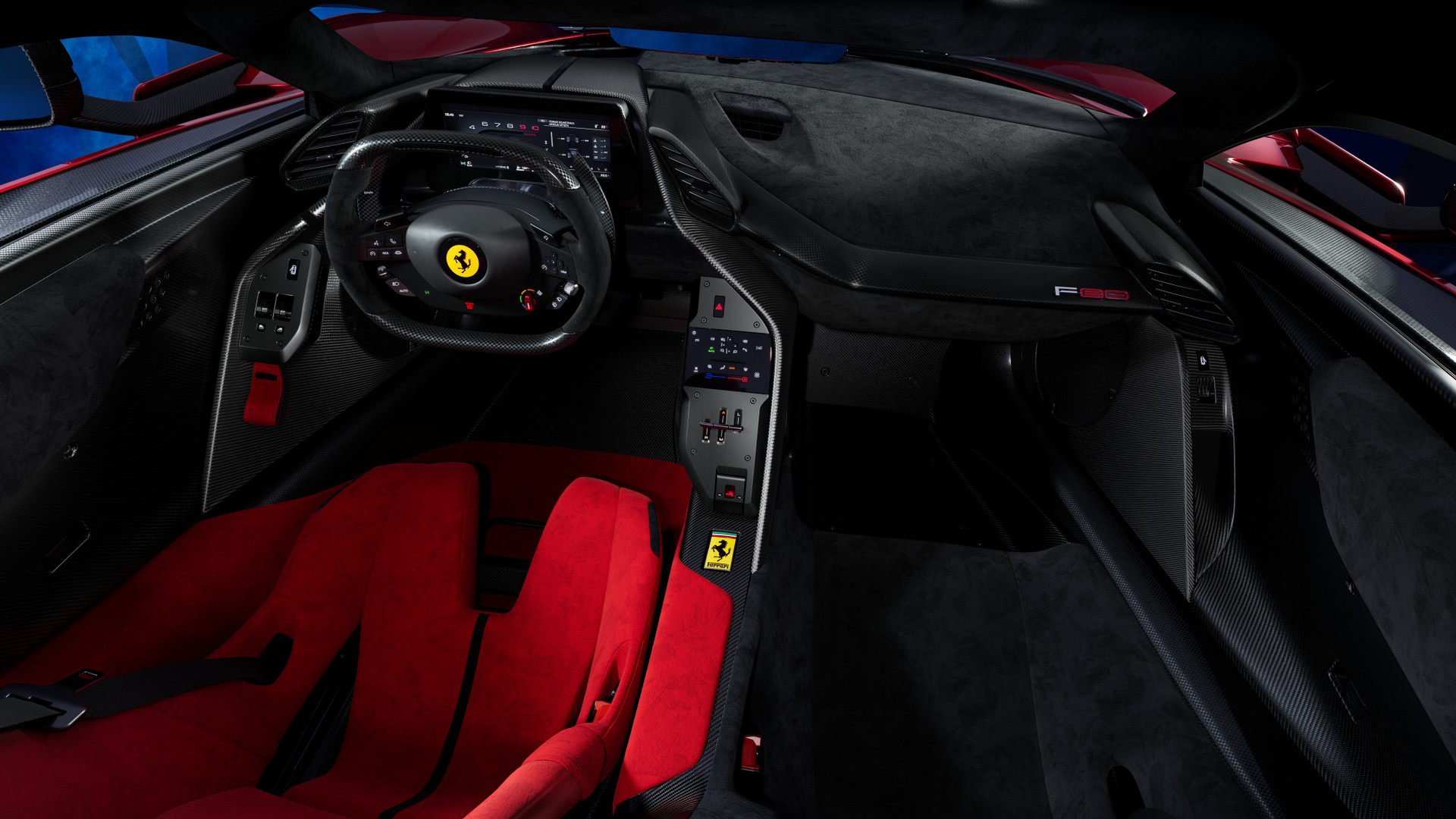
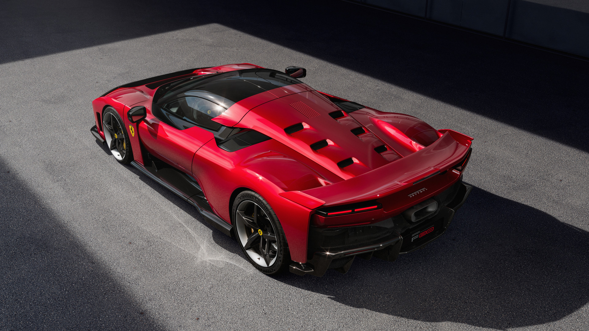
Ferrari has lifted the lid on the most powerful road-going supercar it has ever built, cramming the carbon fibre-laden F80 with a three-liter twin-turbo six cylinder engine that develops 900hp on its own.
The combustion engine is then paired up with three electric motors (all developed in house) that throw an additional 300hp into the mix. That’s 1200 horses in total from a propulsion system that is essentially derived from its 499P Le Mans race car, but is equally as happy popping to the shops for a pint of milk.
Far from an attempt to reduce Ferrari’s overall carbon emissions, this is instead an exercise in extracting maximum performance. The diminutive 800V/2.3kWh battery that is stashed behind the seats, for example, uses F1 technology to ensure it can charge and discharge in the quickest and most efficient way possible.
That means customers won’t be able to drive the F80 in an all-electric mode, but will instead be able to rocket from a standstill to 62mph in 2.15 seconds, reach 124mph in just 5.75 seconds and max out at 217mph. Mind-melting stuff.
(Image credit: Ferrari)
The F80 is engineered for raw performance, using a carbon-fiber chassis that is as narrow as engineers could get away with to ensure less aerodynamic drag. Inside, there’s just about enough room for the driver and one very small passenger.
Ferrari calls it a "1+" vehicle, seeing as the second seat is slightly staggered to allow the controls to envelope the driver. To highlight that this isn't some romantic grand tourer, the driver’s seat is bright red, while the poor passenger has to make do with black... and race harnesses.
There’s so much tech trickery going on underneath the spaceship-style body and butterfly wing doors that engineers from Maranello could easily fill an entire Netflix documentary series with content. The motor-controlled active suspension system, for example, negates the need for anti-roll bars and allows the vehicle to transform from hunkered down track monster to a pliant road ride with ease.
Ferrari has harnessed 3D printing technology to create the suspension wishbones, and also used copious amounts of carbon fiber for its five-spoke alloys wheels and has also introduced some serious software trickery to squeeze the most out of race circuit lap times.
Boost Optimization, which race fans can access in the two high performance driving modes (Performance and Qualify), maps warm-up laps of a favored circuit and then automatically delivers additional horsepower in the section that it deems need it most, such as when accelerating along a straight.
A technological powerhouse
(Image credit: Ferrari)
The Ferrari F80 won’t actually go into production until 2025 – from then, the 799 lucky customers that are selected to receive one will have to wait until 2027 to experience it. Handily that's Ferrari’s 80th anniversary, hence the name.
It will cost around €3.6million, which is over $4million and almost AU$6million, by far the most expensive Ferrari road car ever built and up there with some of most expensive production super cars of all time.
But it moves the game on for the Italian automaker, not just in the raw figures when compared to the LaFerrari it usurps but also in the active aerodynamic technology, track-focussed features and extensive use of e-motors in everything from the turbochargers to the suspension system.
The proof is in the pudding, as the marque claims the F80 posted a new lap record of its Fiorano test track of 1min 15.3secs – that’s 4.4 seconds faster than the LaFerrari.
This might sound like marginal gains, but the numbers are huge in the cutthroat world of low-volume but hideously expensive super cars.
The Sun’s corona, its outermost atmospheric layer, holds the key to understanding solar activity, including phenomena like solar flares and space weather events. For decades, scientists have grappled with the challenge of measuring the Sun’s coronal magnetic field, as this field drives much of the energy that leads to solar eruptions.
Now, in a groundbreaking achievement, Professor Tian Hui's research team from Peking University, in collaboration with international experts, has made the first conventional measurements of the global coronal magnetic field. Their findings, published in the journal Science (Volume 386, No 6717), offer new insights into the Sun’s magnetic activity over a period of eight months.
The Sun’s magnetic field is responsible for storing and releasing energy, which heats the plasma in the corona and triggers solar eruptions. These eruptions, in turn, can have significant impacts on space weather, potentially affecting satellite operations, GPS systems, and even human spaceflight. However, due to the relatively weak nature of the coronal magnetic field compared to the magnetic field on the Sun’s surface (the photosphere), measuring this field has proven to be a significant challenge.
The importance of coronal magnetic field measurements
As the Sun rotates, there are variations in the magnetic fields and the ability to regularly monitor the Sun’s coronal magnetic field will improve our understanding of solar eruptions and help protect high-tech systems on Earth and in space.
Over the years, there have been routine measurements of the photospheric magnetic field, but the coronal field has remained elusive. This limitation has impeded scientists' ability to fully understand the three-dimensional magnetic field structure and the dynamic processes that occur in the Sun’s atmosphere.
In 2020, Tian Hui's team developed a method called “two-dimensional coronal shocks,” which enabled the first measurements of the global distribution of the coronal magnetic field. This was a major milestone, marking a crucial step towards the goal of routine coronal magnetic field measurements.
More recently, Tian's team refined this method further, allowing them to track magnetohydrodynamic shear waves in the corona with greater precision. This made it possible to diagnose the distribution of coronal density and, as a result, determine both the strength and direction of the magnetic field.
Using the Upgraded Coronal Multi-Channel Polarimeter (UCoMP), the research team conducted detailed observations of the Sun’s corona from February to October 2022. Over this eight-month period, they collected 114 magnetograms, or magnetic field images, which allowed them to observe the evolution of the coronal magnetic field at different altitudes and latitudes across multiple solar rotations. The magnetic field strength measured between 1.05 and 1.60 solar radii and varied from less than 1 gauss to around 20 gauss.
With these measurements, they were able to create a global map of the magnetic field intensity in the Sun’s corona. This map revealed how the magnetic field evolves over time and across different regions of the Sun.
When compared to the predictions of the most advanced global coronal models—such as the one developed by Predictive Science, a U.S.-based company—the team found that their observational data closely matched the model’s predictions in mid- and low-latitude regions. However, they noted larger discrepancies in high-latitude regions and active areas of the Sun.
These findings are critical for improving current models of the Sun’s magnetic activity and understanding the dynamics of solar eruptions. As lead author Yang Zihao explains, the team's observations provide a key foundation for refining and optimizing coronal models, which could eventually lead to more accurate predictions of solar eruptions and their potential impact on Earth’s space environment.
This study marks a shift in solar physics, as the field enters a new era of routine coronal magnetic field measurements.
According to Tian Hui, this achievement is just the beginning. While their current methods allow for the measurement of the magnetic field at the edge of the solar disk, the next goal is to develop techniques that will enable a complete measurement of the entire coronal magnetic field, including the solar disk itself. This will require the integration of other measurement methods and tools, but it represents a critical objective for the solar physics community in the coming decades.
Hot on the heels of China’s accusations that Volt Typhoon is actually a CIA asset, a group of cybersecurity experts from the Cyber Security Association of China (CSAC) have now claimed Intel products sold in China contain “frequent vulnerabilities and high failure rates.”
CSAC also said Intel products present “serious risks to national security,” alleging the US semiconductor manufacturers installed an NSA backdoor “in almost all” of its central processing units (CPU) since 2008 to create a “next-generation security defense system.”
“This poses a huge security threat to the critical information infrastructure of countries around the world, including China,” CSAC said as part of its accusations on the organization’s WeChat account.
Push to open investigation
The US and China have frequently thrown similar allegations at each other, with US lawmakers recently pushing for greater restrictions to be placed on suppliers passing US advanced chip manufacturing equipment on to Huawei, which the US placed on its entity list in 2019, restricting businesses from trading with the Shenzhen headquartered technology company.
In a statement posted to WeChat, Intel’s China unit said, “We will maintain communication with the relevant authorities, clarify any concerns, and reaffirm our commitment to product safety and quality” (ViaReuters).
CSAC has also requested the Cyberspace Administration of China launch an investigation into Intel products sold in China for vulnerabilities and backdoors “to effectively safeguard China's national security.”
Stress, cyberthreats and overworking are making cybersecurity professionals want to quit in droves, new research has claimed.
The findings from BlackFrog reveal almost a quarter (24%) of security heads are actively seeking a change of job, with over half (54%) not yet at the quitting point, but open to new opportunities.
Overwhelmingly, stress and demands are the main considerations for security pros looking to quit, with 93% stating these as the main cause of their decision to potentially leave.
Burnout reaching new highs
The report also found CISOs and IT security decision makers are also working overtime in an attempt to keep their business secure, with almost every respondent (98%) stating they work more than their contracted hours.
Of those exceeding their hours, 15% are working more than 16 hours of additional time per week in an attempt to defend against almost constant ransomware and malware attacks. The average security pro was found to put in just over an extra day (9 hours) of work per week.
The reasons given for increased stress mirror the changing threat landscape faced by security professionals, with 42% of respondents voicing their concern about the potential for threat actors to integrate AI tools into their attack vectors, with a quarter of respondents also citing data exfiltration as a top concern. 37% stated the threat of ransomware and malware attacks are a significant source of stress.
When it comes to managing stress, there are some positives. Sport and physical activity is recognized as a means of dealing with stress and complementing overall health, with 86% stating that they allocate time to activities. Sleep, on the other hand, is harder to come by, with only three quarters (75%) stating that they get enough shut-eye.
Despite working significant amounts of overtime, 82% of those surveyed said that they set a clear boundary between their work and private life. The downside however is just under half (45%) have used drugs or alcohol as a way to deal with the pressures of the job, and 69% said that they have been more unsociable.
Help is being offered from the upper management of businesses, with many being offered practical support for dealing with the stress of the job, including flexible hours (64%) and hybrid or remote working for their role (62%).
But security heads still believe that there's more to be done to manage their stress and keep them from quitting, with bigger budgets for security tools (41%) and time prioritization for the things that really matter (40%) stated as additional measures for relieving stress and burden.
As computing shifts from single-chip processors to multi-chip systems, traditional communication methods, such as Network-on-Chip (NoC) and Network-in-Package (NiP), are becoming less efficient. To address these limitations, scientists are exploring terahertz frequencies for high-speed data transfer, despite the challenge of noise interference, which complicates data decoding.
A research team from universities in Australia and the US has been studying wireless communication at the chip level and looking at ways to reduce noise. By applying Floquet engineering, a quantum technique that manipulates electron behavior, they found they were able to improve terahertz signal detection.
When implemented in a two-dimensional semiconductor quantum well (2DSQW), the approach successfully mitigated noise and boosted signal clarity. The team’s findings suggest that this method could pave the way for more effective and reliable wireless communication between chiplets, offering a potential solution for the efficiency challenges faced in multi-chip systems.
Wide-ranging applications
The team also developed a dual-signaling system that uses two receivers to monitor noise levels and adjust signals in real-time, further reducing error rates.
Writing forTech Xplore, researchers Kosala Herath and Malin Premaratne explained, “By overcoming the challenges of noise and signal degradation, our dual-signaling technique marks a key advancement in developing high-speed, noise-resistant wireless communication for chiplets. This innovation brings us closer to creating more efficient, scalable, and adaptable computing systems for the technologies of tomorrow.”
The University of Adelaide has developed a polarization multiplexer that doubles data transmission capacity at terahertz frequencies, while researchers at the University of Notre Dame showcased a silicon topological beamformer chip capable of splitting a single terahertz signal into 54 smaller beams.
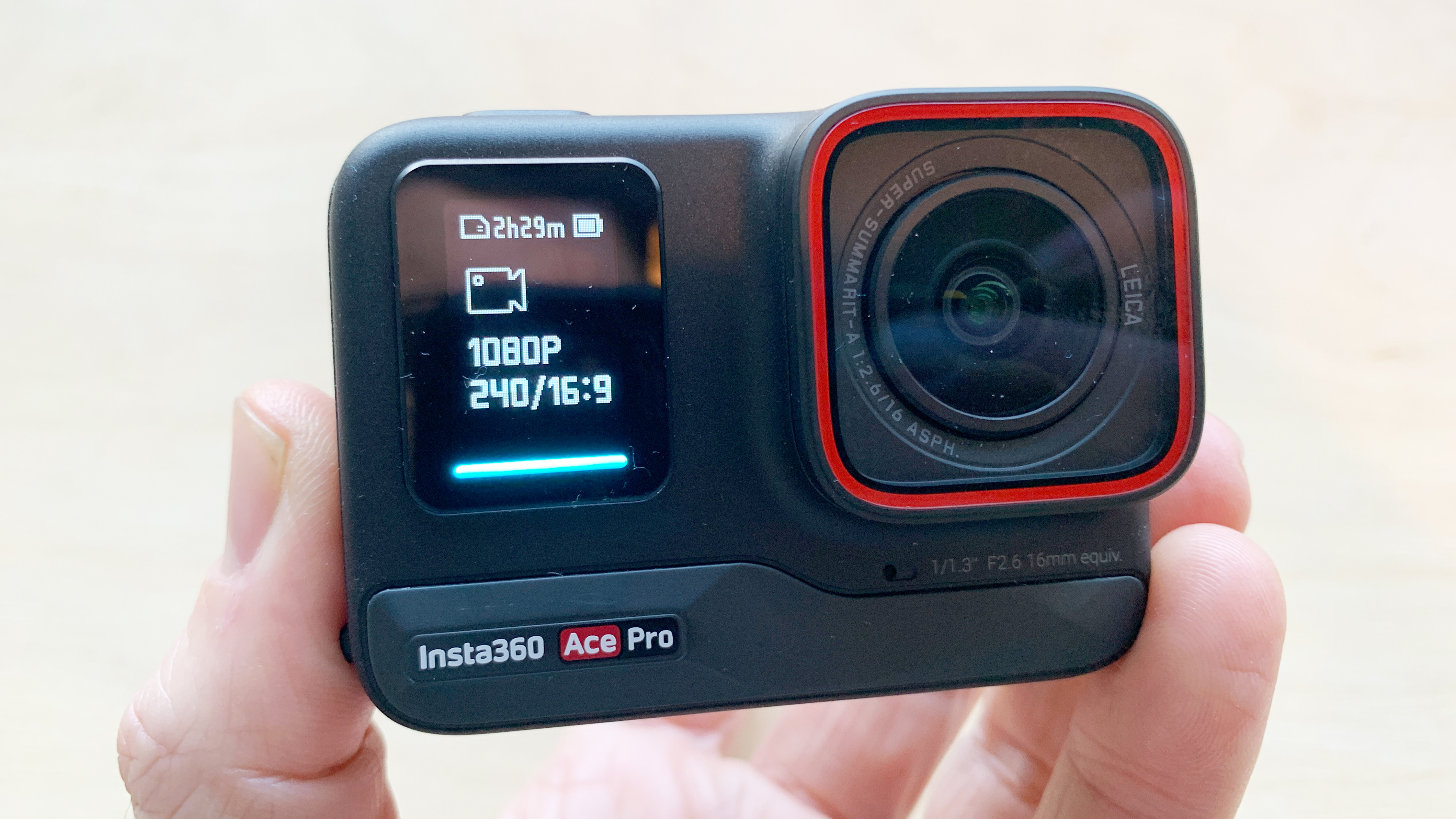
The Insta360 Ace Pro from November 2023 remains the most powerful action camera we've tested, but that looks likely to change soon – according to some leaked marketing materials that spill the beans on a new Ace Pro 2.
As always, the source of these leaks is the reliable @Quadro_News on X (formerly Twitter, below), who's posted some useful slides that give us an idea of what to expect from Insta360's flagship GoPro rival.
Previous leaks had already told us that the Ace Pro 2 is likely to have a 1/1.3-inch main sensor (this time with a 50MP resolution, rather than 48MP). But it seems that the new action cam will pair its 5nm AI chip with some new silicon called the 'Pro Imaging Chip'.
Exactly what the latter does isn't clear, but from the other slides it will seemingly boost software features like PureVideo, which primarily handles low-light performance. From a slide of leaked specs, it seems the Ace Pro 2 will now be able to shoot Active HDR footage at 4K/60p (rather than maxing out at 4K/30p), while PureVideo will now be available for 4:3 clips alongside the usual 16:9 aspect ratio.
👉Our favorite of 2024? A 1/1.3-inch sensor that captures more light, has extended dynamic range and delivers high image quality in conditions unavailable to other action cameras.🤔#insta360 #insta360acepro2 pic.twitter.com/WVuEHo7zvpOctober 12, 2024
Another slide shows Insta360's 'Memories Album', which will seemingly use AI to help organize and potentially edit your clips (a bit like GoPro's Quik app). The PR material separately adds that the action cam "delivers high image quality in conditions unavailable to other action cameras" (no prizes for guessing who Insta360 is referring to).
There's still no news on a release date sadly, but these leaks suggest it'll be worth waiting a week or two if you're about to pull the trigger on a GoPro Hero 13 Black or DJI Osmo Action 5 Pro.
Room for improvement?
(Image credit: Paul Hatton)
So far, it looks like the Insta360 Ace Pro 2 will be a relatively minor upgrade of the Ace Pro – and there's no news yet on if it'll support 10-bit color depth, which Insta360 previously confirmed isn't possible on the current model due to hardware limitations.
That would certainly be a benefit to pro shooters who want to edit their footage or shoot in a 'flat' log profile. But given our Insta360 Ace Pro review called that camera "an absolute monster" without 10-bit video, the feature may not prove to be a deal-breaker for many either way.
The Ace Pro currently sits third in our guide to the best action cameras, with its lofty $449.99 / £429 / AU$729 price tag being one of the few things holding it back from eclipsing GoPro and DJI.
If it could add features like 'log' recording and develop its AI-powered features beyond low-light noise reduction, then it may yet grab that top spot when it launches – hopefully very soon, if these leaks are any sign.
South Korean memory giant SK Hynix has announced it has begun the mass production of the world’s first 12-layer HBM3E, featuring a total memory capacity of 36GB, a huge increase from the previous 24GB capacity in the 8-layer configuration.
This new design was made possible by reducing the thickness of each DRAM chip by 40%, allowing more layers to be stacked while maintaining the same overall size. The company plans to start volume shipments by the end of 2024.
The HBM3E memory supports a bandwidth of 9600 MT/s, translating to an effective speed of 1.22 TB/s if used in an eight-stack configuration. The improvement makes it ideal for handling LLMs and AI workloads that require both speed and high capacity. The ability to process more data at faster rates enables AI models to run more efficiently.
Nvidia and AMD hardware
For advanced memory stacking, SK Hynix employs innovative packaging technologies, including Through Silicon Via (TSV) and the Mass Reflow Molded Underfill (MR-MUF) process. These methods are essential for maintaining the structural integrity and heat dissipation required for stable, high-performance operation in the new HBM3E. The improvements in heat dissipation performance are particularly important for maintaining reliability during intensive AI processing tasks.
In addition to its increased speed and capacity, the HBM3E is designed to offer enhanced stability, with SK Hynix’s proprietary packaging processes ensuring minimal warpage during stacking. The company’s MR-MUF technology allows for better management of internal pressure, reducing the chances of mechanical failures and ensuring long-term durability.
Early sampling for this 12-layer HBM3E product began in March 2024, with Nvidia’s Blackwell Ultra GPUs and AMD’s Instinct MI325X accelerators expected to be among the first to use this enhanced memory, taking advantage of up to 288GB of HBM3E to support complex AI computations. SK Hynix recently rejected a $374 million advanced payment from an unknown company to ensure it could provide Nvidia with enough HMB for its in-demand AI hardware.
“SK Hynix has once again broken through technological limits demonstrating our industry leadership in AI memory,” said Justin Kim, President (Head of AI Infra) at SK Hynix. “We will continue our position as the No.1 global AI memory provider as we steadily prepare next-generation memory products to overcome the challenges of the AI era.”
Windows 11 24H2 has got off to a somewhat wobbly start - with a number of bugs being discovered, though thankfully, there are no huge blunders (yet) - but one thing to be aware of is that the upgrade can take a pretty long time to install.
There’s an official Reddit thread detailing what features and changes users can expect to see with version 24H2 of Windows 11, as well as a FAQ section. And in the latter, Microsoft admits that 24H2 can be very slow going with respect to the time it takes to install.
Microsoft observes: “This is a significantly larger update than the regular monthly updates you have been installing up until now. In some cases, it can take a few hours to install, so be patient! You do not need to babysit it, and you can continue to use your computer during most of the installation.”
So, as noted, you can keep using your PC while the installation process is churning away in the background. Or so Microsoft assures us, anyway, though performance will be affected to some extent at times. And, of course, once the update is ready to go, you will be forced to sit through a whole lot of spinning circles and multiple reboots where you can’t do anything (with your PC, anyway).
(Image credit: Future / James Holland)
What’s the secret of a great installation? Timing
If you want a rough idea of installation times, there’s a report from PC World which tested how long it takes to install Windows 11 24H2 on various laptops. While noting that Microsoft describes 24H2 as a ‘full OS swap’ to underline how noticeably bigger it is than previous updates, PC World recorded installation times varying from just over an hour, to one hour and 45 minutes. Four laptops were tested in total, with the average time taken for those devices being around an hour and a half. So yes, that is longer than most folks are used to - certainly these days anyway.
PC World notes that as you’d expect, as a general rule, older laptops take longer to update, and I echo its recommendation that you set aside some time in your day (an hour or two) if you want to update to version 24H2. Time during which you can at least keep glancing at, and keeping an eye on, your PC while it’s updating.
Windows 11 24H2 is in the process of being rolled out in a phased, gradual manner, and when it’s your device’s turn, the upgrade should be offered automatically. You can keep manually checking for it in Windows Update if you’re keen, though.